An Automatic Test Pattern Generation (ATPG) technique to capture defects in SoC
Abstract
2
Introduction
3
Our approach
7
NaNoINTEGRITY Defect Detection Technique
10
Summary
12
References
13
Nanometer technology scaling pose significant challenges for test engineers working on developing defect-free SoC. Deep nanometer technology designs are always vulnerable to various signal-integrity (SI) issues. In complex System on Chip (SoC) designs, these issues are due to the ever-increasing timing delay variations in the interconnecting networks and gates. Thereby, the chip’s overall performance and power consumption are affected and contribute to a rise in the defective parts per million (DPPM). Supply noise (SN) in the power and ground networks is one factor that increases defects in an SoC. This noise can be eliminated to a great extent by modelling the SI impacts and testing the SoC design with a set of high-quality test patterns that will ensure a better delay defect coverage in designs.We propose a NaNoINTEGRITY Defect Detection Technique in Automatic Test Pattern Generation (ATPG) technique by selecting a set of sensitive victim gate nets, simultaneously inducing all these victim gate nets and generating test patterns under supply noise impact. This technique uses the most effective nets for pattern generation based on the supply noise information determined from the design layout. We have developed this NaNoINTEGRITY Defect Detection Technique by customizing the existing scan-based techniques to capture delay defects by generating supply-noise modelled delay testable patterns. Our effective pattern generation technique is verified in ITC’99 benchmark circuits.
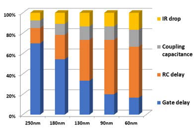
Integrated circuits (ICs) are the vital part of any digital systems. CMOS is a technology used for constructing IC’s. CMOS technology scaling has opened up previously unimaginable opportunities for IC development, delivering higher integration, increased speed, reduced chip size and low power consumption. But they are limited by the increased number of failures that may lead to low product quality of the manufactured products. These failures are due to the integration of billions of transistorson a single piece of silicon. Research studies on VLSI has shown that large portion of IC failures are due to delay defective parts being manufactured. Nowadays, as more transistors are integrated on a single chip, interconnects have become longer and it has an increased impact on path delay. The graph in Fig. 1. shows that withshrinking technolog y node, the percentage of delay caused by coupling effect between signal lines and voltage drop (IR drop) on power and ground lines are taking a larger portion of the delay. These are due to the increased impact of the various physical design issues.
With shrinking technology, the impact of signal integrity issues on SoC designs is increasingly crucial. These SI issues pose significant challenges in the design and testing of complex SoC designs with numerous circuits embedded in them. In a circuit design, SI issues can cause unpredictability in the expected signal outcome. It becomes difficult to model them during the design phase and difficult to capture the defects during the test phase. If these defects are not captured beforehand, the chip’s performance may degrade, which consequently can cause functionality issues in SoC’s. Also, SI issues can increase the number of defective chips going undetected during the test phase, thereby increasing the failure rate in SoC products. Therefore, SI issues have to be thoroughly investigated and SI aware specific models have to be developed and tested for faults in SoC designs. For that, ATPG tools must be capable of identifying, at test phase, the delay faults that can cause potential defects in an SoC.
For good signal integrity, the signal should be of high quality i.e., with less signal voltage drop and current spikes in the supply networks. That is not the case at present. During increased switching activity, current spikes are developed and it gets converted into voltage bounces. Thereby, high currents are drawn from the supply network, causing voltage drop to occur. The reduction in supply voltage reduces the gate’s drive strength which increases the signal delay. Along with voltage drop,the signal timing should be within the estimated timing margin. There should not be any delay in the signal-to-gate arrival time [2], as it might induce delay fault. Sources of SI issues are crosstalk noise [3] in the interconnecting nets, power supply noise (PSN) and ground noise (GN) in the power/ ground distribution network, thermal noise and others. We are focusing here on the inconsistent behaviour of supply noise (SN) and on the unnoticed excessive delay from the impact of SN in thepower and ground networks in an SoC layout.ATPG tools are capable of generating patterns that can capture delay faults. Typically, these tools utilize the synthesized gate level information to minimize the pattern generation time. As it is very difficult and time consuming to determine the noise from synthesized gates, ATPG tools do not take the physical design gate level information from the design layout into consideration. Additional gate delays from the physical design are neglected, so that faulty patterns can be identified morequickly. We can only estimate delays accurately from the geometry of the design’s layout. Therefore, ATPG tools have to generate SN aware delay patterns to capture the maximum number of delay faults. In our work, we employ a path delay fault model based on the gate’s supply networks to identify faults due to SN effects.Usually, in semiconductor industry IC failures are detected during the testing phase after they are manufactured. Fig. 2. shows a sketch of a conventional path delay fault testing where a combinational circuit is under test. A path delay fault test is performed here using a path-delay fault model. The path shown, blue in colour is sensitized to detect a fault. This model is utilized to detect whether the path is too slow because of any faults at their internal nodes. This may even cause circuit failure by introducing an extra delay to the circuit path such as a delayed switching or as false switching. So, detecting these faults has become vital for ensuring better product quality.
In recent years, several analyses conducted on the behaviour of SN and various ATPG techniques to generate delay aware patterns. Authors in [4] proposed pattern generation techniques that considered worst-case timing scenarios in order to find the patterns that create maximum supply noise. In [5], a power supply noise monitor is proposed to prevent signal integrity faults only if excessive PSN is detected. A framework to generate supply noise tolerant delay test patterns considering the IR-drop effects of excessive PSN on the design performance during at-speed test patterns is proposed in [6]. In [7], layout-aware pattern generation procedure with maximum power SN effects on critical paths is proposed. These authors thoroughly considered the SN effects from the design layout and are able to eliminate time consuming pattern validation phase but their proposal lacks practicality in industrial usage. Authors in [8] has substantially addressed the SN effects and proposed noise estimation technique with rigorous testing on critical paths. This may consume higher computational time in generating patterns. In [1], an ATPG technique that generates patternsto test crosstalk noise causing delays is proposed. In this paper, we focus on pattern generation by constraining the victim gate nets that can reproduce the impacts of SN to cause additional delay. We find victim gate nets from the circuit layout for the accuracy in delay estimation. In our work, we modify the existing path delay fault model using an ATPG tool to account for the excess delay from SN impacts.In this paper, we demonstrate that a commercial ATPG tool is not able to identify the worst-case delay patterns causing supply noise defects. Then, we show how an ATPG technique generates supply noise aware delay patterns during at-speed tests using our NaNoINTEGRITY Defect Detection Technique. This ATPG technique can consider any number of victim gate nets surrounding the victim path. For this technique, we utilize an industrial ATPG tool for supply noise aware victim gate selection, modelling and applying different conditions to replicate the issue and then test pattern generation with that. We evaluate our technique for delay variation, using different Integrated circuit (IC) statistical data in HSPICE.Our results also show that an effective pattern can be generated to capture a potential delay defect in lesser time. Our ATPG technique is effective in providing an improved pattern computation and generation time.The remainder of the paper is organized as follows: In the next section we describe an investigatory experiment that shows the delay variations caused by supply noise in the layout of a circuit. Then, we present the detailed flow of our NaNoINTEGRITY Defect Detection Technique that can generate test patterns to detect potential supply noise defects. Finally, we conclude our work in with recommendations for future research.
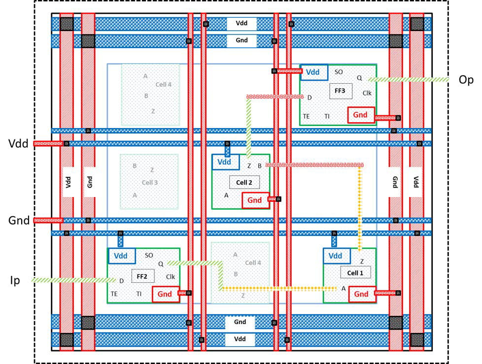
In this section, the motivational goal of our work is presented. Essentially, we aim to show that an existing ATPG tool does not generate high-quality test patterns that can identify SN faults. ATPG tools function on a circuit’s logic level description (i.e., VHDL or Verilog description), so they lack the physical design information while generating patterns. Physical design issues such as power supply noise (PSN) and ground noise (GN) may cause worst-case delays on a circuit path. We separately analyse SN-causing parameters on the power distribution network (PSN) and on the ground distribution network (GN). We estimate their individual impact based on the delay variations in the power/ground networks. Using HSPICE simulations, we identify patterns causing worst-case path delay. Those patterns are then compared with the ATPG tool generated patterns and their discrepancies are compared. From our data, we can infer that an ATPG tool might miss to capture high-quality test patterns if the tool does not consider the physical design parameters causing SN.We perform our analysis and simulations on s27, an ISCAS89 benchmark circuit. s27 circuit is synthesized, DFT scan-chains are inserted and a circuit netlist with gates and flip-flops is generated. Then, placement and routing of the circuit netlist as shown in Fig. 4. is performed to extract the parasitic parameters from the circuit layout. Resistance and coupling capacitance are the parasitic parameters that are extrapolated from the power supply and ground distribution network, as modelled in Fig. 3. Inductance in the power/ground distribution network is not considered in this work, as it may be too complex to analyse its effect on a simple circuit. Usually, in a layout, the power/ground distribution network will be routed through multiple metallic layers, as indicated in red and blue colours in Fig. 4.
The impact of Through Silicon Via’s (TSVs) from different metallic layers are also taken into account. This network model from layout, gives us an accurate delay analysis results in comparison to other simpler models. The CMOS models for the gates/cells are taken from 45nm Predictive Technology Model (PTM) [9]. From the netlist layout,
we can interpret that multiple noise parameters can cause disturbances to the power supply (Vdd) and ground (Gnd) input pins of the gates under observation (victim gate 1/cell 1 and victim gate 2/cell 2); that, too, from different metallic layers.
To test path delay in HSPICE, we consider all of these SN delay causing parameters and then simulate this netlist in the HSPICE tool. The SN delay variations can cause worst-case path delay in circuits, so, we estimate voltage drop at the Vdd and Gnd pins of victim gate 1 and 2, that will experience varying levels of voltage drop with respect to the global supply and ground voltage. For an accurate delay analysis, we also include voltage drop in the interconnecting nets between the standard cells and power/ground pin pads, which are usually ignored during traditional gate level simulations. As interconnects are of varying lengths, the path delay alters to a great extent. This can accurately be estimated based on the power/ground pin pad proximity from the victim gate nets. We identify the voltage drop in the entire victim path from the circuit layout and provide that to the victim gate 1 and 2 for path delay estimation. Also, we provide all the different possible combinations of rising and falling signal transition (vector pair transitions) at FF2 input for the combinatorial victim path in Fig. 3. Vector pair transitions include transitions in the same direction, opposite direction, stable 0 or stable 1 condition at the start of the victim path. The simulation results from the HSPICE tool are then compared with results from an ATPG tool (explained later). Path delays for all input patterns obtained from HSPICE simulations helps us to understand which patterns and under what conditions will provide the worst-case path delay. This will facilitate us to understand the discrepancy in an ATPG tool in generating high-quality test patterns.
We utilize the ATPG tool on s27 circuit to generate path delay test patterns. ATPG is performed on the synthesized, DFT scan-chains inserted netlist using the path delay fault model provided by the tool vendor. The tool does not have a provision to include the SN model or the interconnect models during pattern generation. Basically, they are based on a simplistic model for a faster ATPG. So, it is extremely difficult to identify the exact pattern that can cause SN induced path delay fault. For the ATPG test, we generate patterns for the victim path from FF2/Q to FF3/D, as highlighted in Fig. 5.
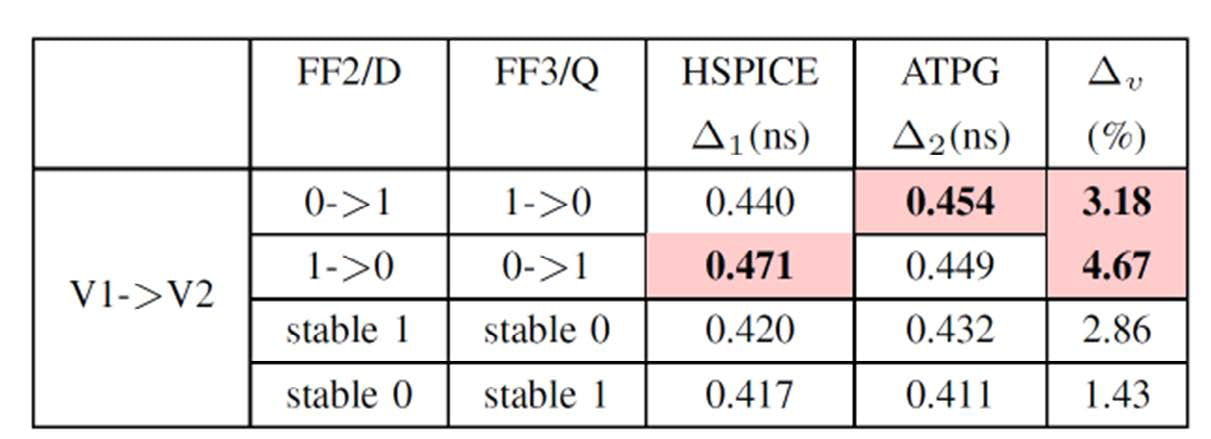
We compare the path delay that we obtain from HSPICE and ATPG simulations. For that, we estimate the path delay variations for 4 input vector pairs (V1, V2) at FF2/D input and observe their output at FF3/Q. In Table I, the input vector pairs (V1,V2) that we provide at FF2/D i.e., {(0,1),(1,0),(1,1),(0,0)} and the output vector pairs that we observe at FF3/Q are respectively shown in column 2 and 3. The path delay we obtain from HSPICE simulation and ATPG simulation i.e., Δ1 and Δ2 are listedin column 3 and column 4. For ATPG simulation, we have not considered SN parameters. The path delay variation Δv is calculated as the mean delay difference between the worst-case delays obtained from HSPICE Δ1 and ATPG Δ2 patterns, calculated using the below equation. From HSPICE, we get the worst-case path delay for vector pair sequence (1,0) and from ATPG we get for (0,1). This input pattern comparison from HSPICE and ATPG simulations shows a clear mismatch.
Also, the path delay variation difference Δv of 4.67% listed in column 6 implies that a high-quality pattern can escape path delay fault testing in ATPG if we do not consider SN parameters during pattern generation. This indicates that we need to re-model the existing path delay fault model in ATPG by including SN impacts. Here, we provide evidence that high-quality patterns are not identified and applied to test delay defects in SoC’s.
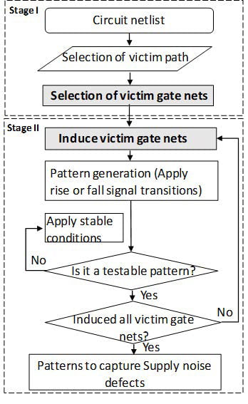
We have developed and implemented this novel NaNoINTEGRITY Defect Detection Technique to capture supply noise defects, as shown in Fig. 6. This technique can generate signal-integrity aware high-quality test patterns for capturing defects inan SoC. This technique consists of 2 major stages. Stage I - Selection of victim gate nets, and Stage II - Inducing victim gate nets based on the signal-integrity impact (here, we have shown for SN impact only) and then pattern generation on the victim path. This technique is implemented, tested and compared with vendor ATPG tool pattern generation and its effectiveness in delay fault testing is validated. Our technique is aimed at capturing the manufacturing defects in an SoC arising due to signal-integrity issues. This technique can be used to characterize the path speed and it helps to address the speed binning problem. Also, they can be employed in improving the classical ATPG technique of pattern generation utilized by any vendor ATPG tool. New page
In this paper, we present an ATPG technique for generating worst-case delay patterns to target path delay faults. The delay fault can be detected under the impact of supply noise induced delay variation in the power supply and ground network for a selected victim net. Our technique is based on inducing all the victim gate nets in the victim path. It does not include the victim gate nets, where the transition signal is propagated and observed for a path delay fault. Our technique can produce similar patterns to the HSPICE delay pattern without performing exhaustive HSPICE simulation method. Our technique is implemented on 12 ITC’99 benchmark circuits and the resultsare shown in comparison to the HSPICE method. By this new technique, we show the effectiveness in CPU runtime and higher pattern quality (can be utilized for SN-aware path delay fault testing).As future work, we plan to extend this technique to combine the effects of signal integrity issues such as crosstalk noise and supply noise-aware pattern generation.
Our NaNoINTEGRITY Defect Detection Technique is aimed at capturing the delay defects in a VLSI chip. This technique can be used to characterize the path speed and it helps to address the speed binning problem. Also, they can be employed in improving the classical ATPG approach of pattern generation utilized in any industrial ATPG tool. The application of our work can bring tremendous improvements to the SoC test quality by ensuring a higher defect coverage and an increased manufacturing yield during speed binning of IC chips.
[1] http://www.techdesignforums.com/practice/technique/parasitics-an-old-problem-reaches-newheights/
[2] A. Asokan et al., “Path delay test in the presence of multi-aggressor crosstalk, power supply noise and ground bounce,” 17th International Symposium on Design and Diagnostics of Electronic Circuits & Systems, 2014, pp. 207-212.
[3] K. Peng, M. Yilmaz, K. Chakrabarty and M. Tehranipoor, “Crosstalk- and Process Variations-Aware High-Quality Tests for Small-Delay Defects,” in IEEE Transactions on Very Large Scale Integration (VLSI) Systems, vol. 21, no. 6, pp. 1129-1142.
[4] A. Krstic, Yi-Min Jiang and Kwang-Ting Cheng, “Pattern generation for delay testing and dynamic timing analysis considering power-supply noise effects,” in IEEE Transactions on Computer-Aided Design of Integrated Circuits and Systems, vol. 20, no. 3, pp. 416-425.
[5] J. R. Vazquez and J. P. de Gyvez, “Power supply noise monitor for signal integrity faults,” Proceedings Design, Automation and Test in Europe Conference and Exhibition, 2004, pp. 1406-1407 Vol.2.[6] N. Ahmed, M. Tehranipoor and V. Jayaram, “Supply Voltage Noise Aware ATPG for Transition Delay Faults,” 25th IEEE VLSI Test Symposium (VTS’07), 2007, pp. 179-186.[7] J. Ma, J. Lee and M. Tehranipoor, “Layout-Aware Pattern Generation for Maximizing Supply Noise Effects on Critical Paths,” 2009 27th IEEE VLSI Test Symposium, 2009, pp. 221-226.[8] M. Chen and A. Orailoglu, “Examining Timing Path Robustness Under Wide-Bandwidth Power Supply Noise Through Multi-Functional-Cycle Delay Test,” in IEEE Transactions on Very Large Scale Integration (VLSI) Systems, vol. 22, no. 4, pp. 734-746, April 2014.[9] Predictive Technology Model (PTM). [Online]. Available:http://ptm.asu.edu/